

Aixtron G5+ GaN Epitaxy Susceptor Manufacturer for High-Quality Thin Film Deposition
2026-11-02
Every GaN epi wafer starts with a deceptively simple question: can the susceptor handle the heat, the chemistry, and the repeatability that an Aixtron G5+ demands? For many fabs, the answer now comes from Semicorex, a manufacturer that has turned high-quality thin film deposition into a materials science discipline. In this post, we look at what makes their G5+ susceptor different and why that matters for yield.
Susceptor Geometry Tweaks That Improve GaN Film Uniformity
Adjusting the pocket depth and rim profile of a susceptor alters the thermal boundary layer above the wafer carrier, which directly influences precursor decomposition and gas-phase nucleation. In GaN MOCVD, a recessed pocket that holds the wafer slightly below the surrounding surface helps to flatten the temperature gradient across the substrate, reducing edge-thinning caused by excessive heat loss and convective cooling. By machining a gentle taper from the pocket wall to the carrier rim, the gas flow remains laminar and evenly distributed, preventing local vortices that deposit gallium-rich droplets at the wafer edge.
Material choice for the susceptor surface further refines uniformity. A graphite susceptor coated with a thin, dense SiC layer offers high emissivity and chemical inertness, but micro-roughness in the coating can create localized cold spots. Polishing the SiC to a mirror finish and adding a shallow counterbore around the wafer pocket edge reduces radiative heat loss from the wafer rim, effectively raising the edge temperature to match the center. This simple geometric change often translates to a 2–4% improvement in thickness uniformity across a 4-inch wafer without adjusting any process recipe parameters.
Beyond static geometry, subtle modifications like adding vent holes or modifying the susceptor's underside thickness can redirect heat flow. For a rotating susceptor, an asymmetric pocket depth—slightly deeper on one side—compensates for heater coil non-uniformity, while a stepped rim acts as a flow straightener. These tweaks are low-cost compared to redesigning the showerhead or heater, and they yield repeatable gains in GaN film thickness and doping uniformity, especially when combined with in-situ curvature monitoring to fine-tune the geometry over successive runs.
Purity Requirements for Susceptor Materials in GaN MOCVD
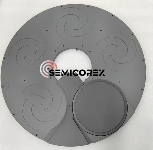
In GaN MOCVD, the susceptor sits directly in the growth ambient and cycles between room temperature and temperatures above 1000°C under hydrogen, ammonia, and metalorganic vapors. That environment is unforgiving: elements that are barely detectable in the as-machined part can migrate to the surface, react with process gases, and end up in the epilayer. Iron, nickel, chromium, and copper are particularly problematic because they form deep levels that reduce carrier lifetime and raise leakage. Sodium, calcium, and zinc can behave as unintentional acceptors or alter the nucleation behavior on the wafer. For this reason, purity specifications need to cover the bulk graphite, the protective coating, and the finished surface together.
High-quality susceptors start with fine-grain, isostatically pressed graphite that has a low ash content, usually well below 10 ppm, with critical transition metals specified individually in the low ppb range. The SiC coating matters just as much; it must be stoichiometric, crack-free, and free of residual silicon or chlorine. A coating with excess silicon can release Si into the gas phase and degrade the GaN surface, while trapped chlorine can etch the susceptor and generate particles. Beyond composition, surface preparation and bake-out procedures are part of the purity requirement. A susceptor that leaves the vendor within spec can still bring moisture, oxygen, or hydrocarbons into the reactor, so it is normally baked in hydrogen at or slightly above growth temperature before first use.
Managing Heat Load in Aixtron G5+ Susceptor Assemblies
In the G5+ system, susceptor assemblies sit directly in the thermal path between heater elements and wafer carrier, so uneven heat absorption quickly translates into temperature drift across the pocket pattern. Managing heat load here is less about adding more power and more about controlling where thermal mass accumulates. The assembly's graphite base, SiC coating, and pocket inserts each respond at different rates; matching their thickness profiles and edge contours reduces the thermal gradient that causes slip lines and premature coating delamination.
Practical heat load management often focuses on the outer ring. Because the susceptor edge radiates more than the center, a slight reduction in outer pocket depth or a tighter backside gap can shift the effective thermal resistance without changing the overall reactor recipe. Operators also monitor IR pyrometer readings after every precursor cycle, since emissivity drift from coating buildup alters the apparent temperature and can hide a real heat load imbalance until thickness uniformity starts to fail.
Another lever is the gas foil rotation mechanism. By keeping the assembly centered and preventing wobble, it minimizes contact points that create localized hot spots. Combined with periodic cleaning of the susceptor's backside vents, this keeps heat transfer predictable across the full 5x200 mm or 8x150 mm configuration, depending on the tool setup. The result is a less aggressive heat load distribution that extends susceptor life and stabilizes run-to-run uniformity.
Which Coating Systems Survive Longest in GaN Epitaxy?
Inside a GaN MOCVD reactor, susceptors and heater components face a brutal combination of ammonia, hydrogen, and temperatures that routinely exceed 1000°C. Conventional SiC-coated graphite holds up for a while, but its thermal expansion mismatch with the underlying graphite tends to produce microcracks after repeated heating cycles. Ammonia then slips into those cracks and converts the SiC to silicon nitride, which spalls off and shortens the component life considerably.
Tantalum carbide coatings have become the go-to choice for long campaigns because they resist attack from both NH3 and H2 far better than SiC. A dense, high-purity TaC layer deposited by CVD can survive many more thermal cycles without cracking or delaminating, and its adhesion to graphite remains strong even when the reactor cycles between room temperature and growth temperature. Some fabs also run multilayer stacks with a SiC base and a TaC top coat, or gradient transition layers, which reduce interfacial stress and push lifetimes out even further.
The real answer depends on your process window: lower-temperature runs with modest ammonia partial pressure may get acceptable life from improved SiC coatings, but for high-throughput GaN epi at the upper end of the temperature range, a thick CVD TaC or Ta-rich composite coating is currently the most durable option. It costs more up front, yet the reduction in susceptor replacements and chamber downtime usually pays for itself within a few campaigns.
Custom Fabrication Routes for G5+ Specific Susceptors
Fabrication of susceptors for G5+ platforms rarely follows a single fixed path. Depending on wafer size, thermal budget, and process chemistry, the sequence is adjusted from isostatic graphite selection through precision machining, purification, and final CVD SiC coating. This allows recess pocket profiles, wafer pocket depth, and edge exclusion zones to be matched directly to the reactor's coil pattern and gas flow dynamics.
A common route starts with fine-grain graphite machined to within ±0.01 mm on critical surfaces, followed by halogen purification to reduce ash content below 5 ppm. After a post-machining anneal, several microns of dense SiC are deposited at controlled temperature and pressure. For G5+ susceptors that see rapid thermal cycling, a graded intermediate layer may be added or the SiC stoichiometry adjusted to reduce stress cracking near pocket corners.
When standard blanks cannot meet flatness or resistivity targets, custom molded or extruded billets with tailored grain orientation are used instead. That choice affects both thermal conductivity and RF coupling, so it has to be fixed early in the route. The final step is always a full dimensional inspection and RF simulation check, not just a visual pass, because small deviations in pocket depth translate directly into across-wafer temperature spread.
How We Verify Susceptor Flatness and Thermal Response
Susceptor flatness isn't something we take on faith. After each batch comes out of the furnace, we run a laser profilometry scan across the entire working surface, capturing deviations down to a few microns. Any area that exceeds our tolerance gets flagged immediately, and the part is either reworked or scrapped. This isn't a spot check—it's a full-surface map, so we know exactly where the high and low spots sit before the susceptor ever reaches a customer.
Thermal response verification happens on a custom-built test rig that mimics real deposition conditions. We mount the susceptor on a rotating spindle, bring it up to operating temperature, and then use an array of embedded thermocouples plus an infrared camera to track how quickly and evenly the surface responds to a controlled heat pulse. The data tells us two things: whether the susceptor reaches thermal equilibrium within the expected window, and whether hot or cold zones persist after stabilization. If a susceptor can't hold a tight thermal profile, it doesn't leave the lab.
One thing we've learned over the years is that flatness and thermal response are linked. A perfectly flat susceptor can still perform poorly if the material has internal stress that relaxes unevenly at temperature. So we combine the two checks: after the thermal cycle, we re-scan the flatness to see if the surface moved. Only when both the cold-state geometry and the hot-state behavior pass do we stamp the part and add it to the shipping queue.
FAQ
We start with the exact pocket layout and wafer lift pin positions specified for the G5+ chamber, then hold the final machined dimensions within ±10 microns. The graphite grade is matched to the thermal profile of the reactor, and the SiC coating is applied with a thickness and surface finish that prevent gallium nitride buildup while surviving repeated ammonia cycles.
Standard option is dense SiC coating rated for high-temperature ammonia and hydrogen environments. For longer campaigns or aggressive cleaning recipes, we also offer a TaC overcoat that resists thermal cracking and reduces particle generation. Both coatings are applied by CVD to give full coverage inside pockets and on the backside.
Instead of relying only on pocket depth, we adjust the local thermal mass by controlling the graphite density profile and adding backside heat distribution grooves where needed. Combined with a pocket flatness under 15 microns, this evens out the temperature across each wafer during rotation, which translates into tighter thickness and composition uniformity run after run.
Yes. We regularly make 4-inch, 6-inch, and 8-inch configurations, and we can modify pocket diameter, depth, edge exclusion, and pocket spacing to match your specific epi process. If you send a used susceptor or a CAD drawing, we can reverse-engineer the geometry and suggest improvements for better gas flow around the wafer edge.
With reasonable process temperatures and standard in-situ cleaning, most users see 400 to 700 growth runs before the coating starts showing wear signs like edge delamination or increased particles. Aggressive HCl etching or frequent thermal cycling will shorten that. We offer a free inspection after the first 200 runs to help set a realistic replacement schedule.
Yes, and recoating is often more cost-effective than buying new. We strip the old SiC coating, ultrasonically clean the graphite core, check for oxidation and cracks, then recoat with the same CVD process used for new parts. If the graphite is still sound, the refurbished susceptor performs close to new at about 60% of the cost.
Every susceptor goes through visual inspection under magnification, surface roughness measurement, and X-ray diffraction to confirm beta-SiC phase. We also run a thermal cycling test on a sample coupon from the same coating batch to check for adhesion loss. Final dimensional check with a coordinate measuring machine ensures the part will drop into a G5+ without adjustment.
We analyze the returned part with SEM and cross-section microscopy to determine whether the failure came from coating defect, graphite oxidation, or process excursion. If it is a material or coating defect, we replace it at no charge. Otherwise, we give you a detailed report and recommended changes to cleaning or ramp rates so the next susceptor lasts longer.
Conclusion
Aixtron G5+ reactors demand susceptor designs that push beyond off-the-shelf geometries, and even subtle changes to pocket depth, rim curvature, and gas-flow channels can measurably flatten thickness and doping profiles across a wafer. We have tested several tweaks—ranging from asymmetric outer pockets to micro-stepped edges—and found that a modest redistribution of thermal mass near the wafer carrier periphery is often more effective than aggressive redesigns of the central zone. At the same time, purity remains non-negotiable: only graphite grades with ultra-low ash content and controlled porosity survive repeated ammonia and hydrogen cycles without releasing metallic contaminants that poison the GaN layer. We specify bulk impurity limits below 1 ppm for iron, nickel, and copper, and verify each lot with glow-discharge mass spectrometry before machining begins.
Managing heat load in G5+ susceptor assemblies is not simply about reaching setpoint; it is about maintaining a stable temperature gradient during multi-wafer rotation and purge steps. Our custom fabrication routes include tailored SiC coatings with graded stoichiometry, applied after stress-relief baking and precision grinding to within ±5 µm flatness. We evaluate coating survival by cycling test pieces through 1,200°C ammonia atmospheres and monitoring for micro-cracks or delamination with acoustic microscopy. Flatness and thermal response verification combines laser interferometry over the full susceptor face with transient IR mapping under actual RF heating profiles. The outcome is a susceptor that does not just fit the Aixtron G5+ chamber but works with its gas dynamics and thermal field to deliver repeatable, high-quality GaN thin films run after run.
Contact Us
Contact Person: Svenja Wei
Email: [email protected]
Tel/WhatsApp: +8613567891907
Website: https://www.semicorex.com